- 您现在的位置:买卖IC网 > Sheet目录983 > HI5960SOICEVAL1 (Intersil)EVALUATION PLATFORM SOIC HI5960
�� �
�
�Application� Note� 9853�
�Appendix� A� Description� of� Architecture�
�The� segmented� current� source� architecture� has� the� ability� to�
�improve� the� converter’s� performance� by� reducing� the�
�amount� of� current� that� is� switching� at� any� one� time.� In�
�traditional� architectures,� major� transition� points� required� the�
�converter� to� switch� on� or� off� large� amounts� of� current.� In� a�
�traditional� 10-bit� R/2R� ladder� design,� for� example,� the�
�midscale� transition� required� approximately� equal� amounts� of�
�currents� switching� on� and� off.� In� a� segmented� current� source�
�arrangement,� transitions� such� as� midscale� become� one� in�
�which� you� simply� have� an� additional� intermediate� current�
�source� turning� on� and� several� minor� ones� turning� off.� In� the�
�case� of� the� HI5760,� there� are� 31� intermediate� current�
�segments� that� represent� the� 5� MSBs� and� ?ve,� binary-�
�Appendix� B� Pin� Descriptions�
�weighted� current� sources� representing� each� of� the� ?ve�
�LSBs.� See� the� Functional� Block� Diagram� in� the� datasheet� for�
�a� visual� representation.� To� relate� the� midscale� transition�
�example� to� the� HI5760,� consider� the� following:� The� code�
�0111111111� would� be� represented� by� 15� intermediate�
�current� segments� and� each� of� the� 5� LSB� current� sources� all�
�turned� on.� To� transition� to� code� 1000000000� would� simply�
�require� turning� off� the� 5� LSB� current� sources� and� turning� on�
�the� next� intermediate� current� segment,� bringing� the� total�
�amount� of� current� switching� at� this� ‘major’� code� transition�
�equal� to� the� same� amount� switching� at� 30� other� code�
�transition� points� in� the� code� ramp� from� 0� to� 1023,� so� that� the�
�total� glitch� energy� is� distributed� more� evenly.�
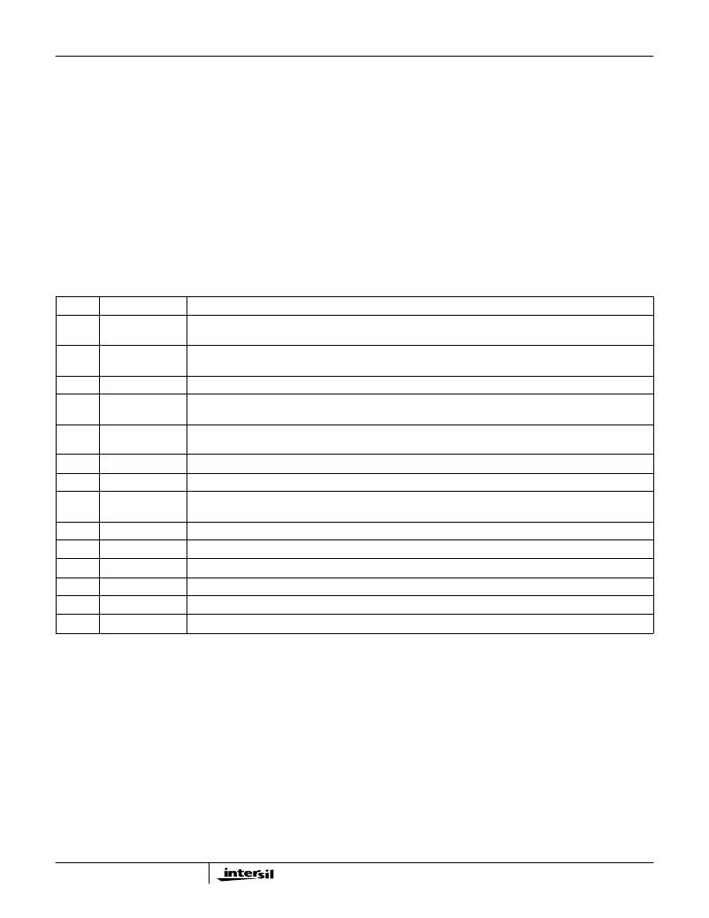
�PIN� NO.�
�1-14�
�15�
�16�
�17�
�18�
�19�
�20,� 25�
�21�
�22�
�23�
�24�
�26�
�27�
�28�
�PIN� NAME�
�D13� (MSB)�
�Through� D0� (LSB)�
�SLEEP�
�REFLO�
�REFIO�
�FSADJ�
�COMP1�
�ACOM�
�IOUTB�
�IOUTA�
�COMP2�
�AV� DD�
�DCOM�
�DV� DD�
�CLK�
�PIN� DESCRIPTION�
�For� the� 14-bit,� HI5960,� these� are� digital� data� bit-13,� (most� significant� bit)� through� digital� data� bit-0,� (least� significant�
�bit).� Pins� 13� and� 14� are� NC� for� the� 12-bit,� HI5860.�
�Control� Pin� for� Power-Down� Mode.� Sleep� mode� is� active� high;� Connect� to� ground� for� normal� mode.� Sleep� pin� has�
�internal� 20� μ� A� active� pull-down� current.�
�Connect� to� analog� ground� to� enable� internal� 1.2V� reference� or� connect� to� AV� DD� to� disable� internal� reference.�
�Reference� voltage� input� if� internal� reference� is� disabled.� Reference� voltage� output� if� internal� reference� is� enabled.� Use�
�0.1� μ� F� cap� to� ground� unless� overdriving� with� a� waveform.�
�Full� Scale� Current� Adjust.� Use� a� resistor� to� ground� to� adjust� full� scale� output� current.� Full� scale� output� current�
�(I� OUTFS� )� =� 32� x� V� FSADJ� /R� SET� ,� (maximum� I� OUTFS� =� 20mA).�
�For� use� in� reducing� noise.� Recommended:� Connect� 0.1� μ� F� from� COMP1� to� AV� DD� .�
�Analog� Ground.�
�The� complementary� current� output� of� the� device.� Full� scale� output� current� is� achieved� when� all� input� bits� are� set�
�to� binary� 0.�
�Current� output� of� the� device.� Full� scale� output� current� is� achieved� when� all� input� bits� are� set� to� binary� 1.�
�Connect� to� ACOM� through� a� 0.1� μ� F� capacitor.�
�Analog� supply� (+3V� to� +5V).�
�Digital� ground.�
�Digital� supply� (+3V� to� +5V).�
�Input� for� clock.� Positive� edge� of� clock� latches� data.�
�3-4�
�发布紧急采购,3分钟左右您将得到回复。
相关PDF资料
HI7188EVAL
EVALUATION PLATFORM HI7188
HI7190EVAL
EVALUATION PLATFORM HI7190
HJ4-L-DC12V
RELAY GEN PURPOSE 4PDT 5A 12V
HL2-HP-AC100V-F
RELAY GEN PURPOSE DPDT 10A 100V
HLM01510Z16K50JJ
RES 16.5K OHM 15W 5% WW
HMC1043-DEMO
DEMONSTRATION BOARD FOR HMC1043
20021311-00034T1LF
集管和线壳 RCPT VT TH
HMC5843-DEMO
BOARD DEMO FOR HMC5843
相关代理商/技术参数
HI5E
制造商:HUBBELL 功能描述:JACK, HI-IMPACT,5E,UNI,YL
HI5E30AA
制造商:Hubbell Premise Wiring 功能描述:
HI5EC
制造商:Hubbell Wiring Device-Kellems 功能描述:JACK, IN-LINE COUPLER,HI,5E,WH
HI-6010
制造商:HOLTIC 制造商全称:Holt Integrated Circuits 功能描述:ARINC 429 TRANSMITTER/RECEIVER FOR 8 BIT BUS
HI-6010_06
制造商:HOLTIC 制造商全称:Holt Integrated Circuits 功能描述:ARINC 429 TRANSMITTER/RECEIVER FOR 8 BIT BUS
HI-6010C
制造商:HOLTIC 制造商全称:Holt Integrated Circuits 功能描述:ARINC 429 TRANSMITTER/RECEIVER FOR 8 BIT BUS
HI-6010CM-01
制造商:HOLTIC 制造商全称:Holt Integrated Circuits 功能描述:ARINC 429 TRANSMITTER/RECEIVER FOR 8 BIT BUS
HI-6010CT
制造商:Holt Integrated Circuits 功能描述:ARINC 429 Transmitter/Receiver 28-Pin SBCDIP